LowPowerCache
Inventions
We started from the consideration low word-size static ram (SRAM) reduces static power and area.

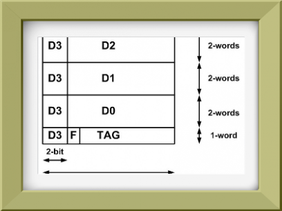
For this reason, we proposed a L1 cache organization mapping the information (TAG,DATA,FLAG) in an unique RAM at reduced word size that keeps unchanged the total capacity of a traditional cache. The unfied data-tag L1 cache SRAM has UA word size and UD address bit. Instead the original cache has two separated SRAM, TAG and DATA; the TAG memory has WT+1 word size (WT bits of tag and 1-bit flag) and WD addess bits. The DATA memory has WA word size and WD+WB address bits, where the WB parameter is address of individual block. The principle of conservation of the total capacity (where possible) is:

This new cache, hereafter unified data-tag cache, could be used both for data and instruction and whichever organization (direct, set-associative and full-associative) and write policies. A prefetch buffer (MINIBLOCK) between the CPU and the L1 unfied cache improve the average access time. Experimental results in 90nm CMOS suggested the area and static power savings of 20% with a penalty of worse average access time by 12%. Below the US patent and the former publication.
G. Visalli and F. Pappalardo "Cache Memory and method with improved mapping flexibility" US 8,250,300
Single Way Cache Organization


